Photonics is a Key Enabling Technology
The International Year of Light, 2015, established under the auspices of the United Nations, aims to strengthen the global awareness of how light-based technologies enforce sustainable development and provide solutions to global challenges in energy, information technologies, education, agriculture, and health. ZIB contributes in particular to nanophotonics research in areas such as solar-energy harvesting and advanced quantum devices, which are key to progress with respect to the global challenges.
Solar Energy
A path with great promise on the road to a clean and sustainable world energy supply is the use of solar energy. Our research follows two paths.
The first one is photovoltaic (PV) energy conversion; the second and new one is artificial photosynthesis. The technology roadmap of the International Energy Agency predicts an annual market of 105 GW for photovoltaic systems in 2030 and a total installed capacity of 900 GW that contributes 5% to the total electricity generation. In view of a sustainable energy supply, these technologies should also not be limited by the abundance of the required materials. This research requires the close collaboration of partners from different fields, and the highlight of 2014’s activities was the opening of the cross-institutional Berlin Joint Lab for Optical Simulations for Energy Research (BerOSE).
Berlin Joint Lab for Optical Simulation for Energy Research (BerOSE)
The lab assists in the research and development of materials and devices for photocatalysis, photovoltaics, and photonics with structure sizes in the nanometer range. The main focus will be the 3-D simulation of both single structures and entire functional systems. The partners of the joint lab are the Helmholtz Center Berlin, the Freie Universität Berlin, and the Zuse Institute, whose specific experience combines experimental and theoretical work and scientific computing. The joint lab is based on a long-term and very successful collaboration of the partners in the field of thin-film photovoltaics. But the lab includes also new research fields: Nanoplasmonics in solar-cells, artificial photosynthesis, and nanophotonic concepts for sensors and functional optical components.

Figure 1 Participants in the grand opening of the Berlin Joint Lab for Optical Simulation for Energy Research.
THIN-FILM SOLAR CELLS: IMPROVING EFFICIENCY WITH LIGHT MANAGEMENT
Silicon thin-film technology has the potential to meet all economic and ecological requirements if the efficiency of solar cells incorporating silicon thin films (today about 12%) can be brought into the range of silicon wafer devices (20-25%). Recent years saw a dramatic breakdown in the industrial production of thin-film cells due to the cheap availability of thicker wafer-based modules. Apart from current industrial considerations, the optimization of thin-film techniques, which are gentle on resources, remains a scientific goal as the gained insight is not limited to solar-cell applications, as it can possibly also be applied, for example, in sensing applications.
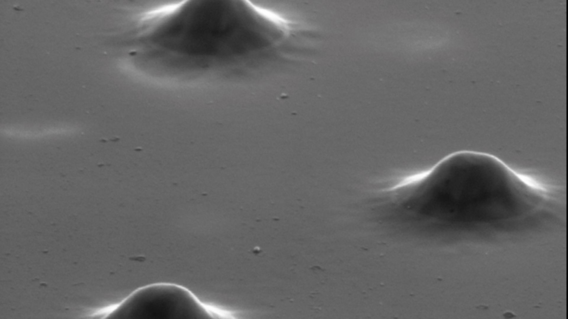
Thin-film devices suffer from insufficient absorption of sunlight in the semi-conductor layer. A promising way of increasing the absorption and thus the efficiency of thin-film solar cells is the use of light-management structures. These textures act as a scattering layer that diffract more of the incident solar irradiation into the absorber layer than a planar material interface. Through total internal reflection, light is kept for as long as possible inside the active semiconductor region of the solar cell, thus enhancing the conversion of photons into electrons. This process is also referred to as “light trapping.“ Figure 2 shows snapshots from different technological approaches to improve light trapping. All of these different concepts have been investigated and optimized with respect to their light-trapping proper ties through means of optical simulation. The classic thin-film approach is to use the naturally occurring random texturing during crystal growth in the production process and optimize it with respect to light scattering (cf. Figure 2a) (FN:Simon Kirner, Martin Hammerschmidt, Christoph Schwanke, Daniel Lockau, Sonya Calnan, Tim Frijnts, Sebastian Neubert, Andreas Schöpke, Frank Schmidt, Jens-Hendrik Zollondz, Andreas Heidelberg, Bernd Stannowski, Bernd Rech, Rutger Schlatmann {2014}. Implications of TCO Topography on Intermediate Reflector Design for a-Si/μc-Si Tandem Solar Cells — Experiments and Rigorous Optical Simulations. IEEE Journal of Photovoltaics, 4, pp. 10-15). Another commonly investigated approach is a periodic arrangement of scattering structures on the metallic back reflector of a solar cell, such as the plasmonic silver nanopyramids shown in Figure 2b). For this simulation, the deposition process of silicon is modeled as well and results in smoother texture. Novel texturing efforts such as nanoimprint lithography can be used to cheaply texture large areas of high-quality silicon. The resulting periodic structures are highly efficient in trapping light and exciting resonances (Figure 2c).
 Random texture in a micromorph tandem solar cell. (b) Armorphous silicon thin film cell on silver pyramid back reflector. (c) Periodic, conical shaped scatterer in etched polycrystalline material.")
Figure 2 Solar cell models for three different types of light scattering elements: (a) Random texture in a micromorph tandem solar cell. (b) Amorphous silicon thin-film cell on silver-pyramid back reflector. (c) Periodic, conical shaped scatterer in etched polycrystalline material.
Artificial Photosynthesis
BerOSE offers new and exciting research topic opportunities in addition to solar-cell light management. Photovoltaic energy conversion relies on sunlight, and the produced electricity cannot be efficiently stored in large quantities today. The most efficient way to store large amounts of energy is in chemical fuels such as gasoline or hydrogen. A novel idea is thus to store solar energy within solar fuels produced through artificial photosynthesis. The goal of artificial photosynthesis is to mimic the green plants in using sunlight to make high-energy chemical solar fuels like hydrogen or ethanol. In close collaboration with our partners Professor van de Krol and Dr. Abdi from the Institute of Solar Fuels at the Helmholtz Center Berlin, we investigate monolithically integrated water-splitting devices. We intend to improve optical absorption within the metal-oxide semiconductor layer with plasmonic effects that also might enhance the catalytic conversion of water to hydrogen and oxygen.
Other Nanophotonics Devices
In addition to solar energy, another focus of our research activities lies in the development of advanced tools for the analysis and design of nanophotonic devices.
Optical Metrology: FinFETs and VNANDs
Optical metrology makes use of the interaction of light with nanostructured objects to measure unknown quantities – most importantly, geometric quantities. Reliable measurements are an essential precondition for any future lithographic manufacturing processes and need to be reliable down to a subnanometer level. In the semiconductor industry, it is used in process control and in mask quality control. Numerical modeling is an important part of optical metrology setups in this field: measurement results are compared to simulation results of a parameterized model in order to quantitatively determine dimensions of the mea-sured sample. With increasing complexity and decreasing feature sizes, the need for accurate optical metrology methods for complex 3-D shapes is increasing (FN:Sven Burger, Lin Zschiedrich, Jan Pomplun, Sven Herrmann, Frank Schmidt {2015}. Hp-finite element method for simulating light scattering from complex 3D structures. Proc. SPIE, p. 94240Z, Vol.9424.).

Figure 3 FinFET: Left: Cross section trough the geometry. Center: Images of parts of the tetrahedral mesh in different viewing directions. Right: Computed reflection spectra for S- and P-polarized light. These spectra are of main interest for the characterization of such components.
Vertical-Cavity Surface-Emitting Lasers (VCSELs)
VCSELs are key components for optical interconnects and are widely applied in high-performance computers and data centers. Single transverse-mode VCSELs are used in sensing, illumination, and display applications. Within this collaboration project, we study designs aiming at large numerical apertures. An example of an excited whispering gallery single-transverse TEM0,49 mode of the cylinder symmetric structure is shown in Figure 2. The field intensity is concentrated along a small circular ring and vanishes in the center. The designed lasers have been fabricated. The 850 nm GaAlAs–based VCSELs demonstrated single-mode lasing and a confirmed operation speed up to 25 Gb/s (FN:Nikolay N. Ledentsov, Jörg-R. Kropp, Vitaly A. Shchukin, Gunther Steinle, Nikolay N. Ledentsov, Jarek P. Turkiewicz, Bo Wu; Qiu Shaofeng, Yanan Ma, Feng Zhiyong, Sven Burger, Frank Schmidt, Christoph Caspar, Ronald Freund, Kent D. Choquette {2015}. High-speed modulation, wavelength, and mode control in vertical-cavity surface-emitting lasers. SPIE OPTO 93810F.).
 and cross section (right)")
Figure 4 Field intensity of a lasing VCSEL. Top view (left) and cross section (right)
Quantum Dots with Lenses
Due to the increasing use of telecommunication in all areas of society, be it political, industrial, or private, potential threats by unwarranted access to data by third parties has become a major source of concern for users as well as providers of communication channels. Great efforts have been made in guarding communication against attacks and eavesdropping; however 100% security cannot be guaranteed in classic transmission systems as the risk of wiretapping or other attacks is always present.
Quantum communication, on the other hand, has the potential of achieving that long-sought-after goal of absolute security, as at its core it relies on the quantum nature of singular particles, which may not be copied or altered without being noticed by the communication partners.
To enable quantum communication, novel, nonclassic light sources are needed which are capable of reliably generating singular quanta of light, a.k.a. photons. In contrast to classic light sources, which are designed to emit as many photons as possible, light sources suitable for quantum communication may only generate one photon at a time to ensure that only one copy of the information the photon carries is in existence.
Our group in collaboration with the Institute for Solid-State Physics of TU Berlin is involved in the optimization of such nonclassic light sources based on quantum dots in GaAs semiconductors. Simulating the optical field in a quantum-dot-based single-photon emitter is a fast, inexpensive, and reliable way of optimizing such devices and gives rise to higher efficiency, better thermal properties, a smaller footprint, and many more technological and economic properties (FN: M. Gschrey, M. Seifried, L. Krüger, R. Schmidt, J. Schluze, T. Heindel, S. Burger, S. Rodt, F. Schmidt, A. Strittmatter, and S. Reitzenstein {2014}. Advanced Quantum Light Sources: Modelling and Realization by Deterministic Nanofabrication Technologies. Advanced Photonics for Communications, OSA Technical Digest, IW1A.).

Figure 5 Left: Numerical model of a single photon emitter device consisting of a Bragg grating and the quantum source covered by a Gaussian lens. Right: Experimentally realized Gaussian lenses.
Optical Chirality
An object is called chiral if it cannot be identified with its mirror image. Chiral objects react differently to left or right circular polarized light. This is called optical activity and is used in many applications. A chiral structure, which can be dispersed in a liquid to investigate interactions with large chiral molecules, can, for example, be achieved by etching a surface that is not symmetric in the sense that it has a crystalline structure with nonstandard orientation. The etching causes chiral cavities in the surface from which negative forms can be extracted and dispersed (see Figure 6). Recently, there has been an interest in studying this kind of artificially manufactured chiral nano-objects to study qualitatively new physical effects on molecules for biological or pharmaceutical applications (FN:Kevin M. McPeak, Christian D. van Engers, Mark Blome, Jong Hyuk Park, Sven Burger, Miguel A. Gosálvez, Ava Faridi, Yasmina R. Ries, Ayaskanta Sahu, and David J. NorrisNamen {2014}. Complex Chiral Colloids and Surfaces via High-Index Off-Cut Silicon. Nano Letters 2014 14, 2934-2940.).

Figure 6 Artificially created chiral nano-structures and the corresponding geometric model
Advances in Adaptive Finite Element Methods
The focus of this algorithmic-oriented research is the generalization and performance improvement of the adaptive finite-elements framework for the solution of Maxwell’s equations. In recent years, we have added a number of new key features.
UNBOUNDED DOMAINS
A key to a rigorous and efficient solution for optical scattering problems is a suitable treatment of wave propagation on unbounded, possibly heterogeneous, exterior domains. During the entire period of our research, we developed and continuously improved a new approach called Pole Condition, and extended a given approach, the Perfectly Matched Layer technique, to cope efficiently with such problem types. Besides Maxwell equations, we extended the concepts to the Schrödinger equation, Klein-Gordon equation, and drift-diffusion equation.
REDUCEDBASIS METHODS
Based on the finite element package, adaptive, error-controlled reduced basis methods for solving parameterized 3-D optical scattering problems have been developed and applied in manifold multi-query and real-time contexts. The main application fields are the optimization of solar-cell structures as well as inverse problems for parameter reconstructions as they occur, for example, in optical metrology.
HIERARCHICAL HIGH-ORDER FINITE ELEMENTS
We completed our software package with hierarchical high-order finite elements for different types of mesh cells (tetrahedrons, hexahedrons, prisms, and pyramids) that can be combined in hybrid meshes. Such hybrid meshes with adaptively chosen mesh size and order are superior to traditional meshes of uniform type and uniform in size and order.
HYDRODYNAMICMODELS IN PLASMONICS
The light-matter interaction, even in classic or semiclassic formulations, gives rise to new physical effects when the structure sizes approach the subwavelength scale. In the range of a very few nanometers, the classic local Drude model has to be replaced by models closer to quantum mechanics. We developed a numerically consistent nonlocal hydrodynamic model that was able to predict the right resonances in nanoparticles.
PERIODICUNBOUNDED DOMAINS
A very recent result involving unbounded domains is the optimization of organic light-emitting diodes (OLED) where we developed novel numerical techniques allowing fast computation of the light outcoupling efficiency. The special situation is that the unbounded simulation domain consists of periodic or quasiperiodic scatters. To account for this horizontal extension of the OLED, we applied a recently proposed technique based on a Floquet transform. This allows for a restriction of the calculations to a unit cell of the periodic structure and results in an enormous gain in the numerical efficiency.