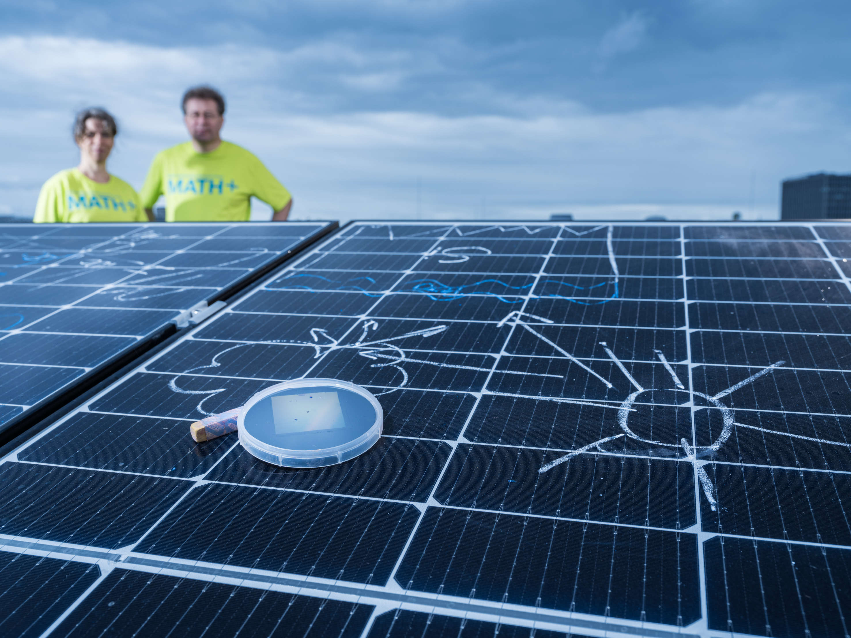
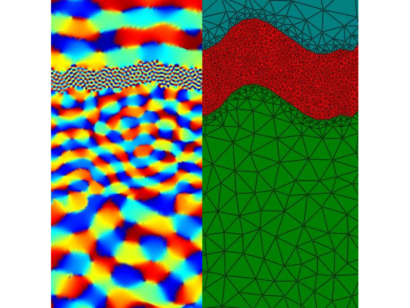
This project aims to advance optical materials for photovoltaics and photonics, with textures on nanometer scales. To do this, we perform rigorous 3D simulations for functional systems and components. The project is a cooperation within the Joint Lab BerOSE which is a laboratory shared by Helmholtz-Zentrum Berlin für Materialien und Energie GmbH (HZB), Freie Universität Berlin (FU) and Zuse Institute Berlin (ZIB). The project profits from the combination of the backgrounds of the various partner institutions in experimental, theoretical and computational research. Specific structures of interest are thin-film silicon photovoltaic cells, multi-junction devices, large-area 2D photonic crystals for sensing applications, and others.

The project is a cooperation within the Joint Lab BerOSE which is a laboratory shared by Helmholtz-Zentrum Berlin für Materialien und Energie GmbH (HZB), Freie Universität Berlin (FU) and Zuse Institute Berlin (ZIB). The project profits from the combination of the backgrounds of the various partner institutions in experimental, theoretical and computational research. Specific structures of interest are thin-film silicon photovoltaic cells, multi-junction devices, large-area 2D photonic crystals for sensing applications, and others.

