The project Electronics of Nanotextured Perovskite Devices is a project within the Partnership Area (PaA) of the Berlin Mathematics Research Center MATH+ (DFG excellence cluster EXC-2046/1, project ID: 390685689), headed jointly by researchers from WIAS (Patricio Farrell), HZB (Christiane Becker, Klaus Jäger), and ZIB (Sven Burger).
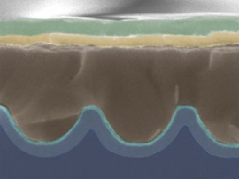
Nanotextured perovskite devices have led to tremendous advancements in various fields, including light emitting diodes and solar cells. For example, at Helmholtz-Zentrum Berlin für Materialien und Energie (HZB) perovskite–silicon tandem solar cells (PSTSC) have been investigated as they allow to overcome the power conversion efficiency limit of conventional silicon solar cells. In recent experiments nanotextured tandem devices, showed various advantages, including smaller reflection losses in comparison to planar tandems, improved electronic material quality of solution-processed perovskite layers, and an increase in fabrication yield.
To a surprising degree the success of nanotextured perovskite–silicon tandem solar cells remains a mystery. It was noted experimentally that the open-circuit voltage for textured cells is higher than for planar cells. While a higher open-circuit voltage is beneficial for device performance, it is not understood theoretically. Understanding the reason is key to further improving the cell design. In contrast to other semiconductor materials such as silicon, in perovskites it is crucial to take ion movement into account.
Hence, the project aims at understanding electronic properties which lead to superior performance of nanotextured perovskite devices such as perovskite–silicon tandem solar cells. We develop real-life 2D/3D charge transport simulations based on drift-diffusion models which include correctly limited ion migration.